
经常会被问到一个问题:为什么做个产品要分这么多个阶段?
POC还没搞完,又来一个EVT;EVT刚跑通,DVT又要开始了。
这些阶段到底是干什么的,能不能跳过几个?
我的回答是:可以跳过,但你大概率付不起那个代价。
产品开发过程中发生的「意外」几乎都是负面的——电源芯片不能正常工作、外壳开模出来跟设计差了三毫米、FCC认证测了三个月测不过。
这些意外不会因为你不走这个阶段就消失,它只会等你上了生产线之后才来,而且来的时候代价已经是指数级的增长了。
产品开发在很大程度上就是一项尽快发现问题的活动。
越早发现问题,代价越小。这个道理大家都懂,但真正做的时候,总觉得自己会是那个例外。
笔者做智能锁产品的时候,一套模具30多万。
样品验证发现问题后还会涉及多次调模,每次调模都至少要一周左右的时间,前后折腾了快三个月才最终稳定。
这就是不走完该走阶段的后果——不是省了时间,是把时间成本转移到了后面,以更高的价格重新付了一遍。
这篇文章,就是要把POC、EVT、DVT、PVT这些阶段说清楚。
每个阶段的目标是什么、交付物是什么、什么时候该停、什么时候该往前推。
帮你在脑子里建一个清晰的路标,别在开发过程里瞎走。
下图的数量仅供参考,不同行业、产品会有区别。

图1:NPI 新产品导入五阶段,红色曲线示意各阶段问题发现成本的变化趋势
POC:验证假设,不是做产品
POC,全称Proof of Concept,概念验证。
这个阶段的核心目标只有一个:用最低的成本,证明你这个产品的核心想法在技术上是可行的。
需要注意的一点是,这个阶段是对技术可行性的确认,不是产品可行性,更不是商业可行性。
很多人在POC阶段就试图把产品做得接近最终形态,结果既浪费了时间,又没得到想要的答案。
POC原型通常是用现成的开发板搭出来的。
Arduino、树莓派、面包板,都是这个阶段的常用工具。
这些东西跟你最后要卖的产品完全不同——它们可能比你的最终产品大十倍、丑十倍,但它们能告诉你:
这个功能能不能实现,用这个传感器能不能达到你想要的精度,这个通信协议能不能稳定工作。
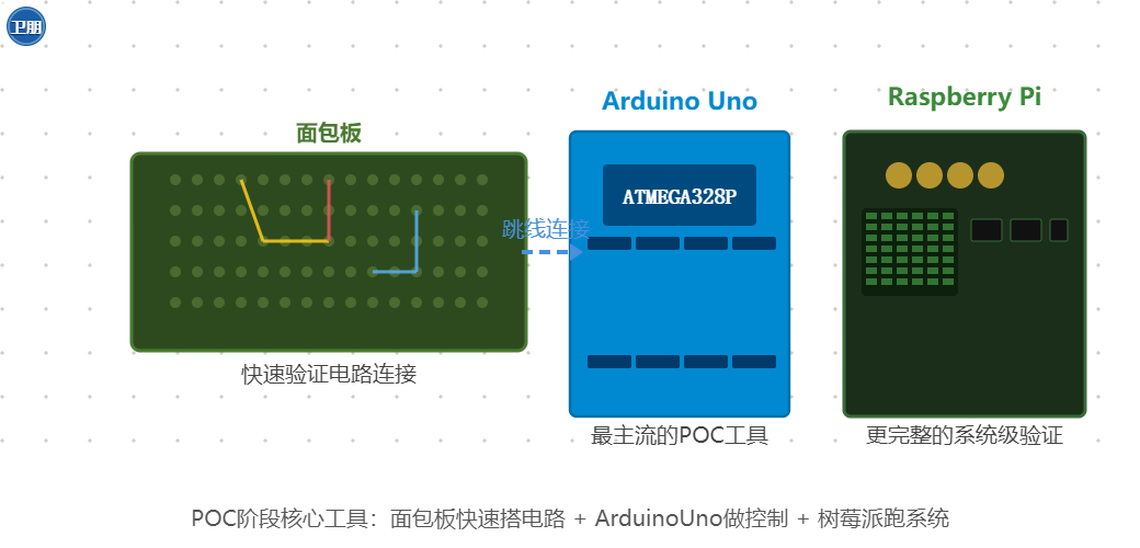
图2:POC 阶段三大常用工具——面包板、Arduino、树莓派
构建POC原型有几条关键原则,笔者认为是这个阶段最重要的:
第一,专注于测试假设,而不是做出产品。
你在POC阶段要验证的,是你对产品最核心的那些技术假设。
比如「用这个蓝牙方案能不能实现十米内稳定开锁」,比如「用这个指纹传感器能不能在0.5秒内完成识别」。
每一个POC回答一个核心问题,问完就停下来。
第二,优先考虑速度,而不是质量。
POC阶段不需要好看,不需要可靠,不需要量产性。
你需要的是快。越快拿到验证结果越好,因为POC阶段的改动成本是整个产品生命周期里最低的。
第三,用现成零件,不要自己造轮子。
这个阶段不是展示你工程能力的时候。能用模块解决的就用模块,能买现成方案的就买现成方案。
你在这个阶段花三个月自己写一个驱动,市场窗口可能已经过去了。
POC阶段客户基本不会看到你的东西。
POC的唯一目的是演示产品创意的核心功能,给内部团队和关键决策者看的。
很多大型科技公司实际上跳过了POC阶段,直接从工程原型开始。
对于那些技术确定性高、团队经验丰富的项目来说,这是合理的。
但如果你对某个关键技术点没有把握,POC是性价比最高的验证方式。
实际上,如果你不具备创建POC的技能,或者对解决方案的可行性没有重大疑问,完全可以跳过POC。
但笔者见到的更多情况是:
团队跳过了POC,然后一头扎进了工程开发,做了半年发现核心技术路线走不通,整个项目推倒重来。
EP工程原型:第一次端到端验证
EP,Engineering Prototype,工程原型。
这个阶段跟POC的区别在于:POC回答的是「能不能」,EP回答的是「合不合理」。
EP样机通常制作不超过5台,主要验证电路原理和核心功能的可行性。
这是硬件设计的第一次端到端验证——从外壳结构到电路板到固件,全部串起来,看能不能跑通。
这个阶段有几个笔者认为特别值得强调的点。
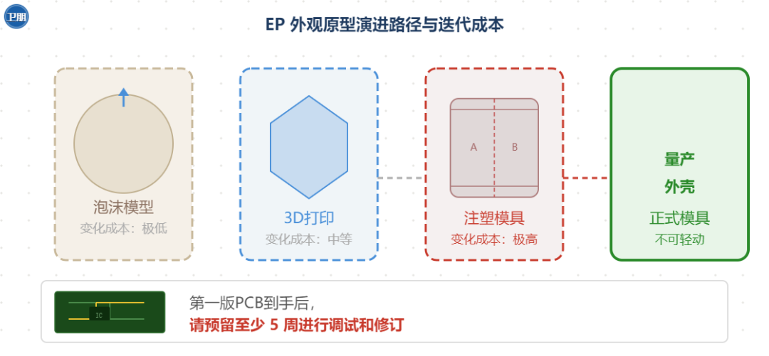
图3:EP阶段外观原型的演进路径——越往后成本越高;以及PCB调试的真实时间预估。
第一,外观的优先级要跟技术同步。
外观原型呈现的是最终产品的外观模型,聚焦在外观、感觉、形式以及产品的美观性上。
对于外观原型,可以使用泡沫、3D打印、CNC加工以及最终注塑等制造技术。
越往后迭代,修改的难度和成本越高。黏土原型的变化很小,3D打印原型的修改程度中等,注塑成型的原型升级则最为复杂——所以在升级原型之前请保持简单,尽可能多学习。
第二,PCB调试要留足时间。
收到最初的PCB原型后,需要对其进行彻底评估,也很有可能需要对其进行修订。
由于你无法提前知道确切的问题,请计划至少五周的时间来调试PCB。
这是一个被严重低估的时间成本。
很多团队以为原理图设计好了PCB打出来就能用,实际上第一版PCB几乎必定需要修改。
第三,塑料外壳是大规模生产最复杂的部分之一。
注塑成型要求遵守非常严格的设计规则,与用于制造塑料原型的3D打印技术完全不同。
3D打印是非常灵活的技术,你可以制作几乎可以想象到的任何形状的塑料原型;而注塑成型要求遵守非常严格的设计规则,包括拔模角度、壁厚均匀、分模线位置等等。
这些东西如果不提前考虑,后面的修模成本会让你睡不着觉。
EVT:把所有设计缺陷暴露干净
EVT,Engineering Validation Test,工程验证测试。
这个阶段的目标是:用20到50台样机,把所有结构、电子和工艺问题暴露干净。
EVT是设计缺陷暴露最多、成本最低的纠错阶段。
在产品开发初期,做改动是比较容易的,随着产品开发阶段向前推进,做改动所要付出的代价呈指数级增长。
EVT阶段每发现一个问题并修复它的成本,大概只有量产阶段的十分之一甚至更低。
EVT单元是使用EP阶段中规定的生产组装程序构建的,包括建立产品的子装配体,然后将它们结合在一起。
EVT单元首次通电后,需要进行一系列功能测试,包括基本功耗测试,还需要确保EVT单元不会过热并且可以承受EMI/静电累积。
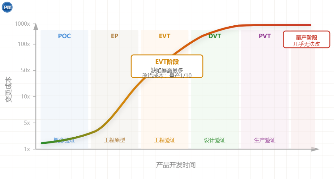
图4:各阶段发现问题并修复的变更成本曲线。EVT是最后一个以低成本集中暴露问题的窗口。
这个阶段有几条硬道理:
第一,EVT的问题多不是团队不行,是这个阶段必然如此。
因为是样品,问题可能较多,往往要经过几轮的样机迭代优化,可能要经历EVT0、EVT1、EVT2等多个EVT周期。
这是正常的,不要因为第一轮问题太多就慌了。
第二,EVT阶段的测试要覆盖生产条件。
不是放在桌上的测试,是放进外壳里测试;不是常温测试,是高低温测试。
测试条件越接近真实生产和使用环境,暴露问题越充分。
DVT:认证必须现在规划,不是以后
DVT,Design Validation Test,设计验证测试。
这个阶段制作50至200台,进一步验证设计的可靠性和可生产性,同时进行认证预测试。
DVT是首次将生产过程作为主要重点,目的是确保产品符合任何必要的法规和环境规格。
DVT设备将经过非常严格的测试,包括跌落、高低温和防水测试。
验证产品的耐用性足以承受日常使用是DVT的主要目标之一。
DVT阶段最容易被初创公司忽视的事情,是认证规划。

图5:DVT 阶段必须启动认证规划的主要标识——FCC、CE、SRRC、CCC、RoHS
电子产品在投放市场之前必须经过各种监管认证。
FCC(美国)、SRRC(中国无线电发射型号核准)、CE(欧盟)、RoHS(环保)——这些认证任何一种都可能花费时间、金钱,甚至可能需要重新设计来获得认证。
一般认证都需要比较长的时间,可能3到8周,能够越早进行越好。
产品设计之初就需要确定所需的认证,并与认证实验室联系以获取报价。
这件事笔者见过太多团队拖到DVT甚至是PVT阶段才想起来搞,结果认证周期严重影响上市时间。
还有一点值得注意:不同国家/地区之间的认证要求差异很大。
刚开始最好将产品限制在一到两个主要市场,以最大程度地减少花费在认证上的时间和金钱。对于有无线功能的产品,使用被认证过的现成模块是一个简化认证过程的有效方式。
另一种获得认证的方式是跟制造商谈判,他们通常拥有内部的专业知识以及必要的测试设备。
认证这件事的核心逻辑是:它不会因为你不管它就消失,你越晚处理它,它的破坏力越大。
DVT阶段是认证规划的最后窗口,再往后就是用钱和时间去买教训了。
PVT:生产线调通之前,不改设计
PVT,Production Validation Test,生产验证测试。
这个阶段制作500台以上,以生产装配工艺验证为主,小规模试产验证量产一致性,是量产前的最后一道关卡。
PVT是第一次正式生产运行,建立一条优先生产线,以优化生产过程。
PVT阶段仅专注于生产,除非出现严重问题,否则绝不会改变产品。
到了这个阶段,设计的改动成本已经高到不可接受,任何设计变更都应该留到下一代产品里去处理。
PVT版本是调整工具和流程的最后机会,该阶段必须开发和测试质量保证(QA)和质量控制(QC)程序。

图6:PVT 阶段必须跑通的四大指标——良率、产能、供应链稳定性、QA/QC 体系
生产中最困难的环节通常不是生产组件,而是把生产需要的所有元器件按期备齐。
供应链上的工作人员面临多个挑战:
元件来自多家供应商,采购者需要跟供应商协商争取一个好价格,某个元件供应商突然中断供货的风险,所用元件都可能被淘汰需要找到合格的可替代元件,元件的交货期不一样,确保元件是正品——这些都必须在PVT阶段验证和解决。
到了PVT阶段,如果良率、产能、供应链还没有跑通,量产就等于自杀。
初创企业通常倾向于完全忽略将其产品从原型扩展到批量生产所面临的复杂性,以及所需的成本和时间。这是最常见的致命错误之一。
笔者见过的那些坑
说到底,这条路上最大的坑有三个。
第一个坑:特征蔓延。
Feature Creep是指项目需求超出原来估计的趋势,尤其对于初创公司,创始人往往对产品充满热情,希望它是完美的,不断添加越来越多的功能。
开发更复杂的产品比开发该产品的简单版本要承担更多的风险——放大了开发成本、时间、推向市场的时间、制造成本,最重要的是放大了风险。
做硬件最忌讳的就是这个。
在POC阶段就锁定核心功能,非核心功能不进BOM。
第二个坑:低估模具成本。
每种定制的塑料件都需要注塑模具,而这些模具成本是将产品推向市场所面临的最昂贵的障碍之一。
以智能锁产品为例,一套模具30多万,尽量减少塑料件的数量会对降低扩展成本产生巨大影响。
这件事在EP阶段就应该是核心关注点,而不是等到EVT才发现外壳方案量产不了。
第三个坑:DFM做得太晚。
从非常早期的开发阶段开始,你就需要考虑如何设计产品以使其易于制造。你越早开始将DFM实践纳入设计,就越容易进行规模制造。
注塑成型的设计规则跟3D打印完全不同,很多团队在EP阶段用3D打印外壳跑通了功能测试,但到了DVT阶段才发现注塑工艺根本实现不了原来的设计,不得不大改结构。
硬件创业失败的快速方法,是输出一堆有缺陷的单元产品。
你投入了大量的时间、精力和资金来使产品投入市场,在制造的早期阶段,你需要尽可能做好充分的质量测试。初创公司的现金流是脆弱的,第一批有缺陷的产品发出去之后,品牌受损加上退货处理,足以让一个还没有稳定现金流的初创公司直接倒闭。
做硬件产品,每走一个阶段都是用钱在买信息。
你在这个阶段花的钱,换来的是对下一阶段风险的更清晰认知。
不要试图省掉这个过程,而是要想清楚:每走一步,我到底要验证什么?
当你对这个问题有清晰答案的时候,POC、EVT、DVT、PVT这些阶段,就不再是流程上的障碍,而是你手里最有力的工具。
A question I get asked often: Why do we need so many phases when developing a product?
The POC isn't even finished, and EVT is already coming; EVT just ran successfully, and now DVT is starting.
What exactly are these phases for, and can we skip some of them?
My answer is: You can skip them, but you'll likely not be able to afford the consequences.
Almost all "accidents" that happen during product development are negative—power ICs failing to work properly, molded housings coming out three millimeters off from the design, FCC certification taking three months and still not passing.
These surprises won't disappear just because you skip a phase; they'll just wait until you're on the production line, and by then the cost will have grown exponentially.
Product development is, to a large extent, an activity to discover problems as early as possible.
The sooner you find a problem, the lower the cost. Everyone understands this, but when it comes to actually doing it, people always think they'll be the exception.
When I worked on smart lock products, a single set of molds cost over 300,000 RMB.
After discovering problems during sample validation, multiple mold modifications were needed. Each modification took at least a week, and it took nearly three months before things finally stabilized.
This is the consequence of not going through the required phases—you don't save time; you shift the time cost to later and pay it back at a higher price.
This article aims to clarify the POC, EVT, DVT, and PVT phases.
The goal of each phase, the deliverables, when to stop, and when to move forward.
Helping you build a clear set of signposts in your mind, so you don't wander aimlessly during development.
The quantities shown below are for reference only; they vary by industry and product.
Figure 1: NPI (New Product Introduction) five-phase model, with the red curve showing the trend of problem discovery cost across each phase.
POC: Verify the Hypothesis, Not Build the Product
POC stands for Proof of Concept.
There is only one core goal for this phase: use the lowest possible cost to prove that the core idea of your product is technically feasible.
One thing to note: this phase confirms technical feasibility, not product feasibility, and certainly not commercial feasibility.
Many people try to make the product near its final form during the POC phase, and end up wasting time without getting the answers they need.
POC prototypes are usually assembled from off-the-shelf development boards.
Arduino, Raspberry Pi, and breadboards are all common tools for this phase.
These things are completely different from the product you'll ultimately sell—they might be ten times larger and ten times uglier—but they can tell you:
whether this feature can be implemented, whether this sensor can achieve the desired accuracy, whether this communication protocol can work stably.
Figure 2: Three commonly used tools in the POC phase—breadboard, Arduino, and Raspberry Pi.
There are several key principles for building POC prototypes, which I consider the most important aspects of this phase:
First, focus on testing hypotheses, not on building a product.
What you need to validate in the POC phase are your core technical assumptions about the product.
For example, "Can this Bluetooth solution achieve stable unlock within ten meters?" or "Can this fingerprint sensor complete identification within 0.5 seconds?"
Each POC addresses one core question, and you stop once it's answered.
Second, prioritize speed over quality.
The POC phase doesn't need to look good, be reliable, or be manufacturable.
What you need is speed. The faster you get validation results, the better, because the cost of changes during the POC phase is the lowest across the entire product lifecycle.
Third, use off-the-shelf components; don't reinvent the wheel.
This phase is not the time to showcase your engineering skills. Use modules whenever possible, and buy off-the-shelf solutions instead.
If you spend three months writing a driver from scratch at this stage, the market window may already have passed.
Customers basically won't see anything from the POC phase.
The only purpose of POC is to demonstrate the core functionality of the product concept, for the internal team and key decision-makers.
Many large tech companies actually skip the POC phase and go straight to engineering prototypes.
For projects with high technical certainty and experienced teams, this is reasonable.
But if you're unsure about a key technical point, POC is the most cost-effective way to validate it.
In fact, if you lack the skills to build a POC or have no major doubts about the feasibility of the solution, you can skip POC entirely.
But what I've seen more often is:
Teams skipping POC, diving headfirst into engineering development, and after half a year discovering the core technical approach doesn't work, forcing a complete restart.
EP (Engineering Prototype): First End-to-End Validation
EP stands for Engineering Prototype.
The difference between EP and POC is: POC answers "can it be done," while EP answers "does it make sense."
EP prototypes are typically no more than five units, mainly validating circuit schematics and core functionality feasibility.
This is the first end-to-end validation of hardware design—from housing structure to PCB to firmware—all connected together to see if it runs.
There are several points in this phase that I believe deserve special emphasis.
Figure 3: Evolution path of appearance prototypes in the EP phase—the later the iteration, the higher the cost; and realistic time estimates for PCB debugging.
First, appearance priority should keep pace with technology.
An appearance prototype presents the exterior model of the final product, focusing on look, feel, form, and aesthetics.
For appearance prototypes, manufacturing techniques such as foam, 3D printing, CNC machining, and final injection molding can be used.
The later the iteration, the more difficult and costly modifications become. Clay prototypes change very little, 3D-printed prototypes have moderate modification scope, and injection-molded prototype upgrades are the most complex—so keep things simple before upgrading, and learn as much as possible.
Second, allow sufficient time for PCB debugging.
After receiving the initial PCB prototype, it needs to be thoroughly evaluated and will likely require revision.
Since you can't know the exact problems in advance, plan for at least five weeks to debug the PCB.
This is a severely underestimated time cost.
Many teams think that once the schematic design is done and the PCB is fabricated, it will just work. In reality, the first PCB version almost always needs modification.
Third, plastic housings are one of the most complex parts of mass production.
Injection molding requires strictly following design rules, which is completely different from 3D printing techniques used to make plastic prototypes.
3D printing is a very flexible technology; you can create almost any shape of plastic prototype you can imagine. Injection molding, however, requires strict adherence to design rules, including draft angles, uniform wall thickness, parting line placement, and more.
If these aren't considered in advance, the mold modification costs later will keep you awake at night.
EVT: Expose All Design Defects
EVT stands for Engineering Validation Test.
The goal of this phase is: use 20 to 50 units to expose all structural, electronic, and process issues.
EVT is the phase where the most design defects are exposed at the lowest cost.
In the early stages of product development, making changes is relatively easy. As the product development progresses, the cost of making changes grows exponentially.
The cost of finding and fixing one problem during EVT is roughly only one-tenth—or even less—of the cost during mass production.
EVT units are built using the production assembly procedures defined in the EP phase, including building product sub-assemblies and then putting them together.
After the EVT unit is powered on for the first time, a series of functional tests are required, including basic power consumption testing, and ensuring the EVT unit won't overheat and can withstand EMI/electrostatic accumulation.
Figure 4: Change cost curve for discovering and fixing problems at each phase. EVT is the last window to expose problems at low cost.
There are several hard truths for this phase:
First, having many issues during EVT doesn't mean the team is incompetent—that's inevitable for this phase.
Since these are prototypes, there may be many issues. They often require several rounds of iteration and optimization, going through EVT0, EVT1, EVT2, and multiple EVT cycles.
This is normal. Don't panic just because the first round has too many problems.
Second, EVT testing must cover production conditions.
Not benchtesting, but testing inside the housing; not room temperature testing, but high and low temperature testing.
The closer the test conditions are to real production and usage environments, the more problems will be exposed.
DVT: Certification Must Be Planned Now, Not Later
DVT stands for Design Validation Test.
This phase produces 50 to 200 units to further validate design reliability and manufacturability, while also conducting certification pre-testing.
DVT is the first phase where the production process becomes the primary focus, ensuring the product meets all necessary regulatory and environmental specifications.
DVT units will undergo rigorous testing, including drop tests, high/low temperature tests, and waterproof tests.
Verifying that the product is durable enough to withstand daily use is one of the main objectives of DVT.
The thing most easily overlooked by startups in the DVT phase is certification planning.
Figure 5: Key indicators for initiating certification planning during the DVT phase—FCC, CE, SRRC, CCC, RoHS
Electronic products must pass various regulatory certifications before being launched to market.
FCC (USA), SRRC (China radio equipment type approval), CE (EU), RoHS (environmental)—any one of these certifications can consume time and money, and may even require redesign.
Certifications generally take considerable time, possibly 3 to 8 weeks, so the earlier the better.
The required certifications should be determined at the beginning of product design, and certification labs should be contacted for quotes.
I've seen too many teams remember to handle this only during DVT or even PVT, and the certification cycle severely impacts time-to-market.
Another point worth noting: certification requirements vary significantly across different countries/regions.
It's best to limit the product to one or two major markets initially, to minimize time and money spent on certification. For products with wireless functionality, using pre-certified off-the-shelf modules is an effective way to simplify the certification process.
Another way to obtain certification is to negotiate with manufacturers, who typically have internal expertise and the necessary testing equipment.
The core logic of certification is: it won't disappear just because you ignore it. The later you deal with it, the more destructive it becomes.
The DVT phase is the last window for certification planning; anything after that means buying lessons with money and time.
PVT: Don't Change the Design Until the Production Line Is Running
PVT stands for Production Validation Test.
This phase produces 500 or more units, primarily focusing on production assembly process validation. Small-batch trial production verifies mass production consistency, serving as the final checkpoint before mass production.
PVT is the first formal production run, establishing a priority production line to optimize the production process.
The PVT phase focuses solely on production. Unless there are serious issues, the product design will never be changed.
By this stage, the cost of design changes has become unacceptably high. Any design changes should be saved for the next generation of products.
The PVT version is the last opportunity to adjust tools and processes. QA (Quality Assurance) and QC (Quality Control) procedures must be developed and tested during this phase.
Figure 6: Four key metrics that must be validated in the PVT phase—yield rate, capacity, supply chain stability, QA/QC system
The most difficult part of production is usually not manufacturing components, but ensuring all components needed for production are available on schedule.
Supply chain staff face multiple challenges:
Components come from multiple suppliers; purchasers need to negotiate good prices with suppliers; the risk of a component supplier suddenly cutting off supply; components becoming obsolete and needing qualified substitutes; varying lead times for different components; ensuring components are genuine—all of these must be validated and resolved during the PVT phase.
By the PVT phase, if yield rate, capacity, and supply chain aren't working, mass production is equivalent to suicide.
Startups tend to completely ignore the complexity and the required cost and time involved in scaling their product from prototype to mass production. This is one of the most common fatal mistakes.
Pitfalls I've Seen
In the end, there are three biggest pitfalls on this path.
First pitfall: Feature creep.
Feature creep refers to the trend of project requirements exceeding original estimates. Especially for startups, founders are often passionate about their product and want it to be perfect, constantly adding more and more features.
Developing a more complex product carries more risks than developing a simpler version—it amplifies development costs, time, time-to-market, manufacturing costs, and most importantly, risk.
This is the biggest taboo in hardware development.
Lock down core features during the POC phase; non-core features don't go into the BOM.
Second pitfall: Underestimating mold costs.
Every custom plastic part requires an injection mold, and these mold costs are one of the most expensive obstacles to bringing a product to market.
Taking smart lock products as an example, a single set of molds costs over 300,000 RMB. Minimizing the number of plastic parts can have a huge impact on reducing expansion costs.
This should be a core focus during the EP phase, not discovered during EVT when the housing solution turns out to be unmanufacturable.
Third pitfall: DFM done too late.
From the very early stages of development, you need to consider how to design the product for manufacturability. The earlier you incorporate DFM practices into your design, the easier it will be to scale manufacturing.
Injection molding design rules are completely different from 3D printing. Many teams use 3D-printed housings to pass functional tests during the EP phase, only to discover during DVT that the injection molding process can't achieve the original design, forcing a major structural redesign.
A fast way for hardware startups to fail is to ship a batch of defective products.
You've invested significant time, effort, and capital to bring the product to market. In the early stages of manufacturing, you need to do thorough quality testing. Startup cash flow is fragile. After the first batch of defective products is shipped, the combination of brand damage and return processing can be enough to bankrupt a startup that hasn't yet stabilized its cash flow.
In hardware product development, every phase is bought with money.
The money you spend in each phase buys you a clearer understanding of the risks in the next phase.
Don't try to skip this process; instead, think clearly about: what exactly am I validating by taking this step?
When you have a clear answer to this question, POC, EVT, DVT, and PVT are no longer obstacles in the process—they become the most powerful tools in your hands.
Original link: https://mp.weixin.qq.com/s/P7D0nEkqlEmlimUDZP2xGA